JEE MAIN 2023 · 30 JAN S1Logic gates and digital circuitsTRANSCRIBED
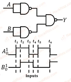
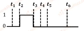
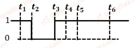
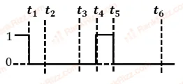
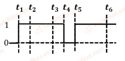
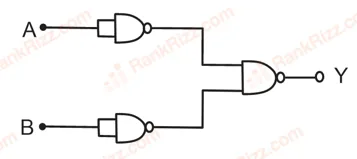
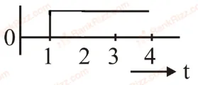
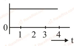
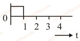
The output waveform of the given logical circuit for the following inputs and as shown below, is
- A
- B
- C
- D
Every Semiconductor Electronics question JEE Main has set, grouped by the idea it tests rather than the order of the syllabus. 253 questions across 5 distinct ideas. Free to read, answer key on every one.
Questions
253
Distinct ideas
5
Share of marks
4.4%
Difficulty
EASY
A chapter is not one subject — it is a handful of procedures the examiner reuses. These are the ones Semiconductor Electronics questions actually test.
81–100 OF 253 · NEWEST FIRST
The output waveform of the given logical circuit for the following inputs and as shown below, is
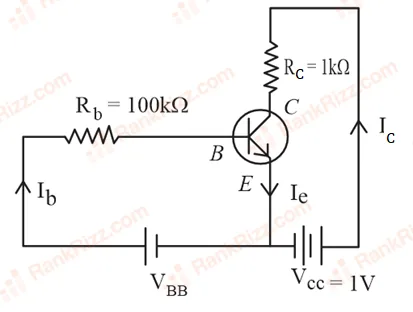
For a given transistor amplifier circuit in CE configuration V, k, k and . Value of base current is
A
A
A
A
Given below are two statements: one is labelled as Assertion A and the other is labelled as Reason R
Assertion A: Diffusion current in a p-n junction is greater than the drift current in magnitude if the junction is forward biased.
Reason R: Diffusion current in a p-n junction is from the n-side to the p-side if the junction is forward biased.
Both A and R are correct but R is NOT the correct explanation of A
A is correct but R is not correct
A is not correct but R is correct
Both A and R is correct and R is the correct explanation of A
Match the List I with List II
A. Intrinsic Semiconductor I. Fermi-level near valence band
B. n-type semiconductor II. Fermi-level at middle of valence and conduction band
C. p-type semiconductor III. Fermi-level near conduction band
D. Metals IV. Fermi-level inside conduction band
(A) I, (B) II, (C) III, (D) IV
(A) II, (B) I, (C) III, (D) IV
(A) II, (B) III, (C) I, (D) IV
(A) III, (B) I, (C) II, (D) IV
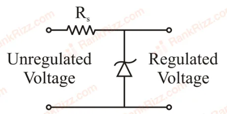
A zener diode of power rating 1.6 W is to be used as voltage regulator. If the zener diode has a breakdown of 8 V and it has to regulate voltage fluctuating between 3 V and 10 V. The value of resistance for safe operation of diode will be
10
12
13.3
13
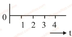
For the logic circuit shown, the output waveform at Y is
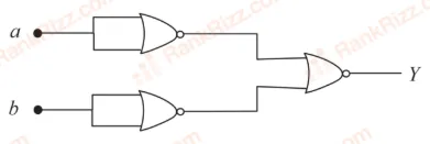
The logic performed by the circuit shown in figure is equivalent to
AND
NOR
OR
NAND
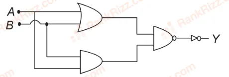
The logic operations performed by the given digital circuit is equivalent to:
NOR
AND
OR
NAND
Statement I: When a Si sample is doped with Boron, it becomes P type and when doped by Arsenic it becomes N-type semi conductor such that P-type has excess holes and N-type has excess electrons.
Statement II: When such P-type and N-type semi-conductors, are fused to make a junction, a current will automatically flow which can be detected with an externally connected ammeter.
In the light of above statements, choose the most appropriate answer from the options given below.
Both Statement I and statement II are incorrect
Statement I is incorrect but statement II is correct
Both Statement I and statement II are correct
Statement I is correct but statement II is incorrect
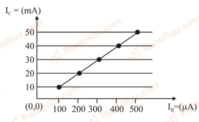
From the given transfer characteristic of a transistor in CE configuration, the value of power gain of this configuration is , for k, and k. The value of is _____.
In the following circuit, the correct relation between output () and inputs and will be
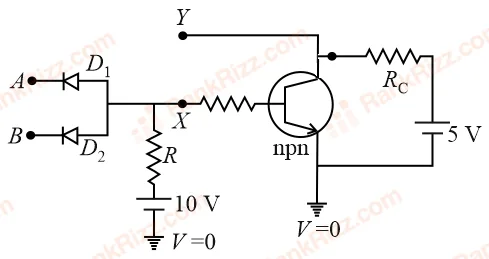
For using a multimeter to identify diode from electrical components, choose the correct statement out of the following about the diode
It is two terminal device which conducts current in both directions.
It is two terminal device which conducts current in one direction only
It does not conduct current gives an initial deflection which decays to zero.
It is three terminal device which conducts current in one direction only between central terminal and either of the remaining two terminals
The photodiode is used to detect the optical signals. These diodes are preferably operated in reverse biased mode because
fractional change in majority carriers produce higher forward bias current
fractional change in majority carriers produce higher reverse bias current
fractional change in minority carriers produce higher forward bias current
fractional change in minority carriers produce higher reverse bias current
Identify the logic operation performed by the given circuit
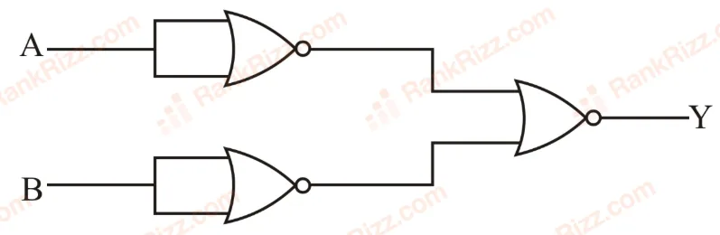
AND gate
OR gate
NOR gate
NAND gate
The I - V characteristics of a junction diode in forward bias is shown in the figure. The ratio of dynamic resistance, corresponding to forward bias voltage of V and V respective is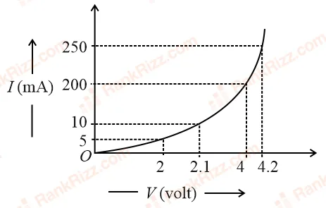
The positive feedback is required by an amplifier to act as an oscillator. The feedback here means
External input is necessary to sustain ac signal in output.
A portion of the output power is returned back to the input.
Feedback can be achieved by LR network.
The base-collector junction must be forward biased.
For a transistor to act as a switch, it must be operated in
Active region
Saturation and cut-off region
Cutoff region only
Saturated region only
Given below are two statements : One is labelled as Assertion A and the other is labelled as Reason R.
Assertion A : transistor permits more current than a transistor.
Reason R : Electrons have greater mobility as a charge carrier.
Both A and R true, and R is correct explanation of A.
Both A and R are true but R is NOT the correct explanation of A.
A is true but R is false.
A is false but R is true.
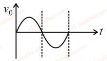
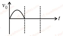
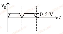
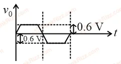
In the given circuit the input voltage is shown in figure. The cut-in voltage of junction diode ( or ) is 0.6 V. Which of the following output voltage () waveform across the diode is correct?
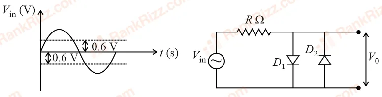
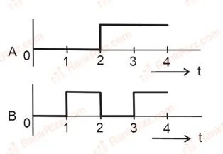
A logic gate circuit has two inputs and and output . The voltage waveforms of , and are shown. The logic gate circuit is
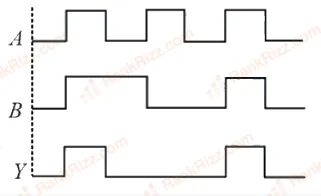
AND gate
OR gate
NOR gate
NAND gate
OTHER PHYSICS CHAPTERS