JEE MAIN 2006Transistors (older syllabus)TRANSCRIBED
In a common base mode of a transistor, the collector current is for an emitter current of . The value of the base current amplification factor will be
- A
48
- B
49
- C
50
- D
51
Every Semiconductor Electronics question JEE Main has set, grouped by the idea it tests rather than the order of the syllabus. 253 questions across 5 distinct ideas. Free to read, answer key on every one.
Questions
253
Distinct ideas
5
Share of marks
4.4%
Difficulty
EASY
A chapter is not one subject — it is a handful of procedures the examiner reuses. These are the ones Semiconductor Electronics questions actually test.
241–253 OF 253 · NEWEST FIRST
In a common base mode of a transistor, the collector current is for an emitter current of . The value of the base current amplification factor will be
48
49
50
51
If the lattice constant of this semiconductor is decreased, then which of the following is correct?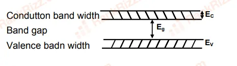
All decrease
All increase
, and increase but decreases
, and decrease increases
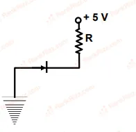
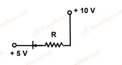
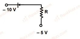
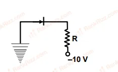
In the following, which one of the diodes is reverse biased?
The circuit has two oppositely connect ideal diodes in parallel. What is the current following in the circuit?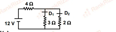
1.33 A
1.71 A
2.00 A
2.31 A
The electrical conductivity of a semiconductor increases when electromagnetic radiation of wavelength shorter than nm is incident on it. The band gap (in eV) for the semiconductor is
eV
eV
eV
eV
In a common base amplifier, the phase difference between the input signal voltage and output voltage is
In a full wave rectifier circuit operating from Hz mains frequency, the fundamental frequency in the ripple would be
Hz
Hz
Hz
Hz
The thermistors are usually made of
metals with low temperature coefficient of resistivity
metals with high temperature coefficient of resistivity
metal oxides with high temperature coefficient of resistivity
semiconducting materials having low temperature coefficient of resistivity.
A piece of copper and another of germanium are cooled from room temperature to K, the resistance of
each of them increases
each of them decreases
copper decreases and germanium increases
copper increases and germanium decreases
The manifestation of band structure in solids is due to
Heisenberg's uncertainty principle
Pauli's exclusion principle
Bohr's correspondence principle
Boltzmann's law
When npn transistor is used as amplifier
electrons move from base to collector
holes move from emitter to base
electrons move from collector to base
holes move from base to emitter
For a transistor amplifier in common emitter configuration having load impedance of k ( and ) the current gain is
When p-n junction diode is forward biased
the depletion region is reduced and barrier height is increased
the depletion region is widened and barrier height is reduced
both the depletion region and barrier height reduced
both the depletion region and barrier height increased
OTHER PHYSICS CHAPTERS