RankRizzStart free

Semiconductor Electronics — JEE Main Previous Year Questions

Every Semiconductor Electronics question JEE Main has set, grouped by the idea it tests rather than the order of the syllabus. 253 questions across 5 distinct ideas. Free to read, answer key on every one.

Questions

253

Distinct ideas

5

Share of marks

4.4%

Difficulty

EASY

The ideas inside Semiconductor Electronics

A chapter is not one subject — it is a handful of procedures the examiner reuses. These are the ones Semiconductor Electronics questions actually test.

01Semiconductors: energy bands, intrinsic and extrinsicset 9×
02p-n junction diode and its characteristicsset 102×
03Diode circuits and rectifiersset 14×
04Zener diode, LED, photodiode and solar cellPractice questions coming soon
05Logic gates and digital circuitsset 85×
06Transistors (older syllabus)set 43×

Every Semiconductor Electronics question

1–20 OF 253 · NEWEST FIRST

JEE MAIN 2026 · 28 JAN S2Logic gates and digital circuitsTRANSCRIBED

Two p-n junction diodes are connected as shown in figure. A and B are input signals and C is the output. The given circuit will function as a________.
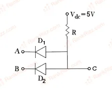
image
  1. A

    NAND Gate

  2. B

    NOR Gate

  3. C

    AND Gate

  4. D

    OR Gate
JEE MAIN 2026 · 23 JAN S1p-n junction diode and its characteristicsTRANSCRIBED

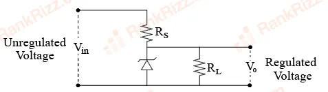
The following diagram shows a Zener diode as a voltage regulator. The Zener diode is rated at and the desired current in load is 5 mA. The unregulated voltage source can supply upto 25 V. Considering the Zener diode can withstand four times of the load current, the value of resistor (shown in circuit) should be ____ Ω .

27
  1. A

    10

  2. B

    4000

  3. C

    100

  4. D

    1000

JEE MAIN 2026 · 21 JAN S2p-n junction diode and its characteristicsTRANSCRIBED

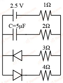
The charge stored by the capacitor C in the given circuit in the steady state is ______ .

30 Slot 2
  1. A

    7.5

  2. B

    5

  3. C

    10

  4. D

    12.5

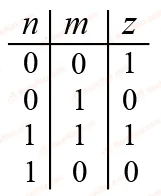
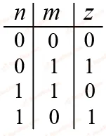
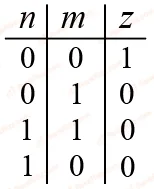
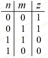
JEE MAIN 2026 · 24 JAN S2Logic gates and digital circuitsTRANSCRIBED

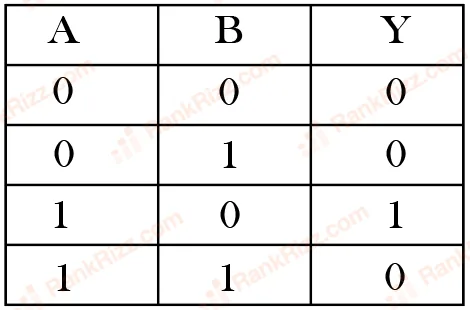
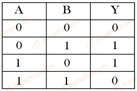
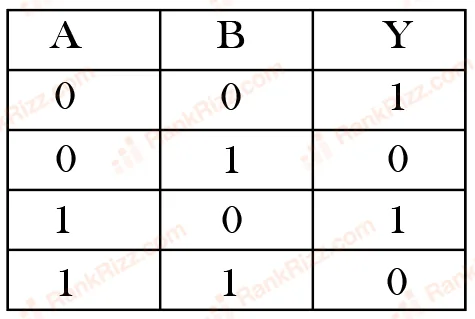
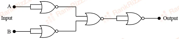
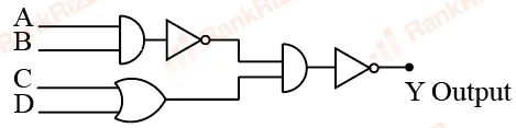
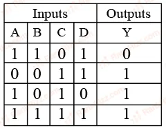
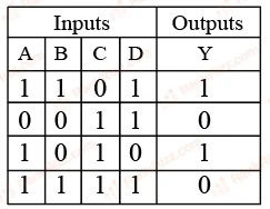
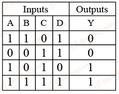
Identify the correct truth table of the given logic circuit.

image
  1. A
    image
  2. B
    image
  3. C
    image
  4. D
    image
JEE MAIN 2026 · 21 JAN S1Logic gates and digital circuitsTRANSCRIBED

The given circuit works as:

Screenshot_3
  1. A

    OR gate

  2. B

    NOR gate

  3. C

    NAND gate

  4. D

    AND gate

JEE MAIN 2026 · 22 JAN S1Logic gates and digital circuitsTRANSCRIBED

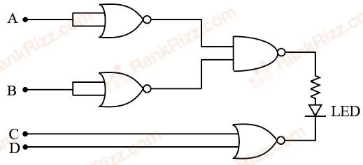
Find the correct combination of A, B, C and D inputs which can cause the LED to glow.

Screenshot_35
  1. A

    1000

  2. B

    0011

  3. C

    0100

  4. D

    1101

JEE MAIN 2026 · 02 APR S2Logic gates and digital circuitsTRANSCRIBED

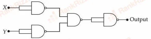
If X and Y are the inputs, the given circuit works as :

image
  1. A

    OR gate

  2. B

    AND gate

  3. C

    NAND gate

  4. D

    NOR gate

JEE MAIN 2026 · 02 APR S1p-n junction diode and its characteristicsTRANSCRIBED

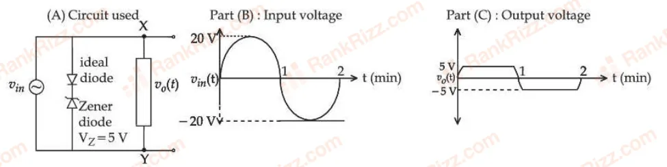
For the given circuit (shown in part (A)) the time dependent input voltage and corresponding output are shown in part (B) and part (C), respectively. Identify the components that are used in the circuit between points X and Y.

image
  1. A
    image
  2. B
    image
  3. C
    image
  4. D
    image
JEE MAIN 2026 · 04 APR S1Logic gates and digital circuitsTRANSCRIBED

Two 4 bits binary numbers, and are given in the inputs of a logic circuit shown in figure below . The output will be :

image
  1. A

  2. B

  3. C

  4. D

JEE MAIN 2026 · 22 JAN S2Logic gates and digital circuitsTRANSCRIBED

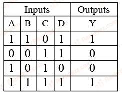
The correct truth table for the given input data of the following logic gate is:

39
  1. A
    39(A)
  2. B
    39(B)
  3. C
    39(C)
  4. D
    39(D)
JEE MAIN 2026 · 06 APR S1p-n junction diode and its characteristicsTRANSCRIBED

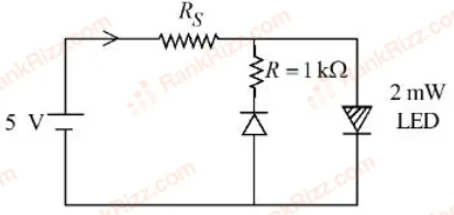
The maximum rated power of the LED is 2 mW and it is used in the circuit with input voltage of 5 V as shown in the figure below. The current through resistance is 0.5 mA.
The minimum value of the resistance of , to ensure that the LED is not damaged is _______ k.

image
  1. A

    6

  2. B

    2

  3. C

    4

  4. D

    5

JEE MAIN 2026 · 28 JAN S1p-n junction diode and its characteristicsTRANSCRIBED

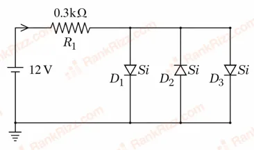
Assuming in forward bias condition there is a voltage drop of 0.7V across a silicon diode, the current through diode in the circuit is ___ mA.
(Assume all diodes in the given circuit are identical)

40-1
  1. A

    18.8

  2. B

    17.6

  3. C

    11.7

  4. D

    20.15

JEE MAIN 2026 · 23 JAN S2Logic gates and digital circuitsTRANSCRIBED

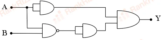
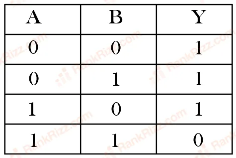
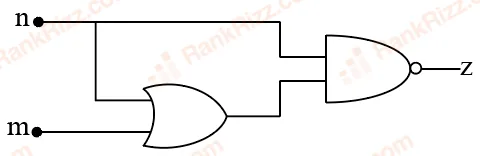
For the given logic gate circuit, which of the following is the correct truth table?

41
  1. A
    41(1)
  2. B
    41(2)
  3. C
    41(3)
  4. D
    41(4)
JEE MAIN 2026 · 04 APR S1p-n junction diode and its characteristicsTRANSCRIBED

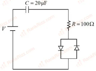
Consider a circuit consisting of a capacitor (20 F), resistor (100 ) and two identical diodes as shown in figure. The resistance of diode under forward biasing condition is 10 . The time constant of the circuit is s. The value of is :

image
  1. A

  2. B

  3. C

  4. D

JEE MAIN 2026 · 06 APR S2Logic gates and digital circuitsTRANSCRIBED

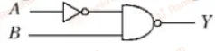
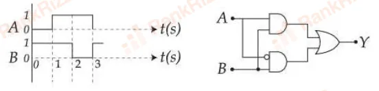
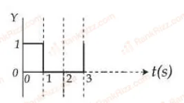
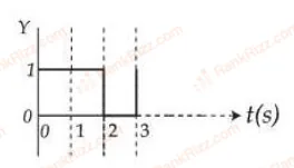
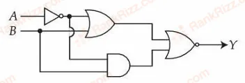
Refer to the logic circuit given below. For two inputs and , output (Y) will be __________.

image
  1. A

    1, 0 respectively

  2. B

    0, 1 respectively

  3. C

    0, 0 respectively

  4. D

    1, 1 respectively

JEE MAIN 2026 · 04 APR S2p-n junction diode and its characteristicsTRANSCRIBED

Given below are two statements: one is labelled as Assertion A and the other is labelled as Reason R

Assertion A: A diode under reverse-biased condition provides very small current which is nearly independent of voltage until a critical limit at which the current increases drastically.

Reason R: Below the critical voltage limit, only majority charge carriers flow which increases drastically above critical voltage.
Choose the correct answer from the options given below : 

  1. A

    Both A and R are true, and R is the correct explanation of A

  2. B

    Both A and R are true, but R is NOT the correct explanation of A

  3. C

    A is true but R is false

  4. D

    A is false but R is true

JEE MAIN 2026 · 05 APR S2p-n junction diode and its characteristicsTRANSCRIBED

In a semiconductor p-n  diode, the doping concentrations on p-side has atoms/cm³ and the n-side has atoms/cm³respectively.  Which one of the following statements is true?

  1. A

    Widths of depletion region on either side of the interface are equal 

  2. B

    The depletion region widths is more on p-side compared to that in n-side

  3. C

    The depletion region width is more on n-side compared to that the p-side

  4. D

    No depletion region forms because of unequal doping concentrations on p and n-sides

JEE MAIN 2026 · 08 APR S2Logic gates and digital circuitsTRANSCRIBED

The output for the given inputs and to the circuit is :

image
  1. A
    image
  2. B
    image
  3. C
    image
  4. D
    image
JEE MAIN 2026 · 05 APR S1Logic gates and digital circuitsTRANSCRIBED

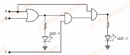
For the given logic circuit, which of the following inputs combination will make both LED-1 and LED-2 to glow?

image
  1. A

  2. B

  3. C

  4. D

JEE MAIN 2026 · 04 APR S2p-n junction diode and its characteristicsTRANSCRIBED

A diode has Zener voltage of 10 V and maximum power dissipation of 0.5 W, then the minimum resistance to be used in series with this diode for safety when it is connected to a 25 V power supply is ______ .