RankRizzStart free

Semiconductor Electronics — JEE Main Previous Year Questions

Every Semiconductor Electronics question JEE Main has set, grouped by the idea it tests rather than the order of the syllabus. 253 questions across 5 distinct ideas. Free to read, answer key on every one.

Questions

253

Distinct ideas

5

Share of marks

4.4%

Difficulty

EASY

The ideas inside Semiconductor Electronics

A chapter is not one subject — it is a handful of procedures the examiner reuses. These are the ones Semiconductor Electronics questions actually test.

01Semiconductors: energy bands, intrinsic and extrinsicset 9×
02p-n junction diode and its characteristicsset 102×
03Diode circuits and rectifiersset 14×
04Zener diode, LED, photodiode and solar cellPractice questions coming soon
05Logic gates and digital circuitsset 85×
06Transistors (older syllabus)set 43×

Every Semiconductor Electronics question

181–200 OF 253 · NEWEST FIRST

JEE MAIN 2019 · 09 JAN S2p-n junction diode and its characteristicsTRANSCRIBED

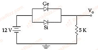
Ge and Si diodes start conducting at 0.3 V and 0.7 V respectively. In the following figure if Ge diode connection are reversed, the value of changes by: (assume that the Ge diode has large breakdown voltage)
  1. A

    0.8 V

  2. B

    0.4 V

  3. C

    0.2 V

  4. D

    0.6 V

JEE MAIN 2019 · 11 JAN S2p-n junction diode and its characteristicsTRANSCRIBED

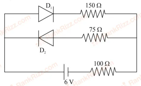
The circuit shown below contains two ideal diodes, each with a forward resistance of . If the battery voltage is 6 V, the current through the resistance (in Amperes) is:

  1. A

    0.036

  2. B

    0.02

  3. C

    0.027

  4. D

    0.03

JEE MAIN 2019 · 10 JAN S1Logic gates and digital circuitsTRANSCRIBED

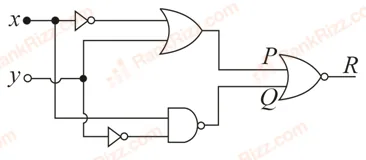
To get output '1' at R, for the given logic gate circuit the input values must be:

  1. A

  2. B

  3. C

  4. D

JEE MAIN 2019 · 12 JAN S2Transistors (older syllabus)TRANSCRIBED

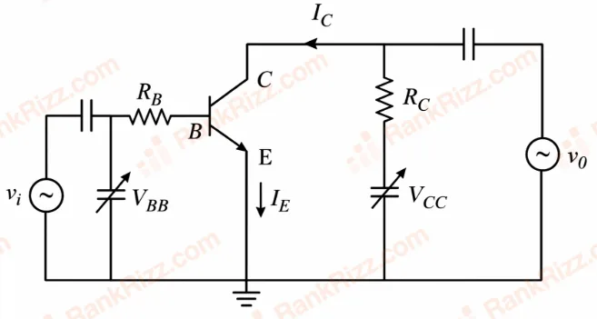
In the figure, given that supply can vary from 0 to 5.0 V, V, , k, k and V. The minimum base current and the input voltage at which the transistor will go to saturation, will be, respectively:

image
  1. A

    and 2.8 V

  2. B

    and 2.8V

  3. C

    and 3.5V

  4. D

    and 3.5V

JEE MAIN 2019 · 12 APR S2p-n junction diode and its characteristicsTRANSCRIBED

Figure shows a DC voltage regulator circuit, with a Zener diode of breakdown voltage = 6 V. If the unregulated input voltage varies between 10 V to 16 V, then what is the maximum Zener current?

  1. A

    1.5 mA

  2. B

    3.5 mA

  3. C

    7.5 mA

  4. D

    2.5 mA

JEE MAIN 2019 · 08 APR S1p-n junction diode and its characteristicsTRANSCRIBED

The reverse break down voltage of a Zener diode is 5.6 V in the given circuit.

image

The current I through the Zener is:

  1. A

    10 mA

  2. B

    7 mA

  3. C

    17 mA

  4. D

    15 mA

JEE MAIN 2019 · 08 APR S2Transistors (older syllabus)TRANSCRIBED

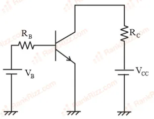
A common emitter amplifier circuit, built using an NPN transistor, is shown in the figure. Its dc current gain is 250, k and V. The minimum base current for to reach saturation is:

image
  1. A

    10 A

  2. B

    40 A

  3. C

    7 A

  4. D

    100 A

JEE MAIN 2019 · 09 APR S1Transistors (older syllabus)TRANSCRIBED

An NPN transistor is used in common emitter configuration as an amplifier with 1 k load resistance. Signal voltage of 10 mV is applied across the base-emitter. This produces a 3 mA change in the collector current and 15 A change in the base current of the amplifier. The input resistance and voltage gain are:

  1. A

    0.33 k, 1.5

  2. B

    0.67 k, 300

  3. C

    0.67 k, 200

  4. D

    0.33 k, 300

JEE MAIN 2019 · 12 APR S1Logic gates and digital circuitsTRANSCRIBED

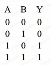
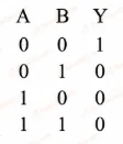
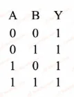
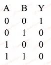
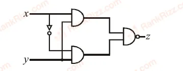
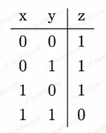
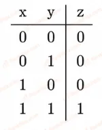
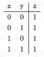
The truth table for the circuit given in the figure is:

  1. A
    image
  2. B
    image
  3. C
    image
  4. D
    image
JEE MAIN 2019 · 10 JAN S2p-n junction diode and its characteristicsTRANSCRIBED

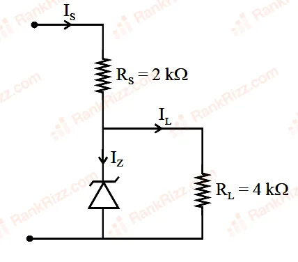
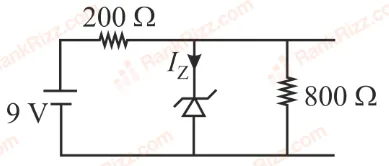
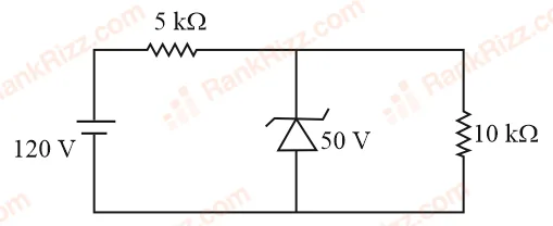
For the circuit shown below, the current through the Zener diode is:

  1. A

    zero

  2. B

    5 mA

  3. C

    9 mA

  4. D

    14 mA

JEE MAIN 2019 · 09 APR S2Logic gates and digital circuitsTRANSCRIBED

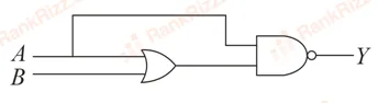
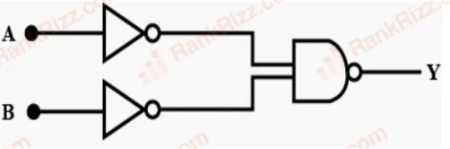
The logic gate equivalent to the given logic circuit is:

image
  1. A

    NAND

  2. B

    AND

  3. C

    NOR

  4. D

    OR

JEE MAIN 2019 · 12 APR S2Transistors (older syllabus)TRANSCRIBED

In a CE transistor amplifier, the audio signal voltage across the collector resistance of 2 kΩ is 2 V, if the base resistance is 1 kΩ and the current amplification of the transistor is 100 then the input signal voltage is

  1. A

    10 mV

  2. B

    1 mV

  3. C

    0.1 V

  4. D

    1 V

JEE MAIN 2019 · 10 APR S2p-n junction diode and its characteristicsTRANSCRIBED

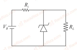
The figure represents a voltage regulator circuit using a Zener diode. The breakdown voltage of the Zener diode is 6 V and the load resistance is, R = 4 kΩ. The series resistance of the circuit is R = 1 kΩ. If the battery voltage V varies from 8 V to 16 V, what are the minimum and maximum values of the current through Zener diode?

  1. A

    0.5 mA; 6 mA

  2. B

    1 mA; 8.5 mA

  3. C

    0.5 mA; 8.5 mA

  4. D

    1.5 mA; 8.5 mA

JEE MAIN 2019 · 12 APR S1Transistors (older syllabus)TRANSCRIBED

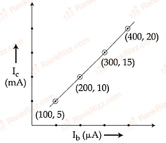
The transfer characteristic curve of a transistor, having input and output resistance 100 Ω and 100 kΩ respectively, is shown in the figure. The voltage and power gain, are respectively:

  1. A

    ,

  2. B

    ,

  3. C

    ,

  4. D

    ,

JEE MAIN 2018 · 15 APR S1Transistors (older syllabus)TRANSCRIBED

In a common emitter configuration with suitable bias, it is given than is the load resistance and is small signal dynamic resistance (input side). Then, voltage gain, current gain and power gain are given, respectively, by: [ is current gain, , , are respectively base, collector and emitter currents]

  1. A

  2. B

  3. C

  4. D

JEE MAIN 2018 · 08 APR OFFLINETransistors (older syllabus)TRANSCRIBED

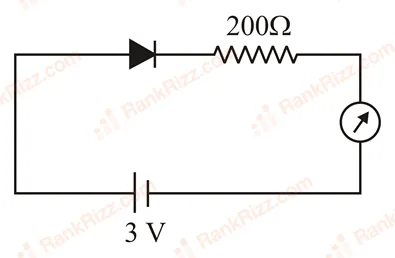
The reading of the ammeter for a silicon diode in the given circuit is:

  1. A

    13.5 mA

  2. B

    0

  3. C

    15 mA

  4. D

    11.5 mA

JEE MAIN 2018 · 15 APR S2Logic gates and digital circuitsTRANSCRIBED

Truth table for the given circuit will be:

  1. A
    image
  2. B
    image
  3. C
    image
  4. D
    image
JEE MAIN 2018 · 16 APR ONLINEp-n junction diode and its characteristicsTRANSCRIBED

In the given circuit the current through zener diode is:

  1. A

    3.3 mA

  2. B

    2.5 mA

  3. C

    5.5 mA

  4. D

    6.7 mA

JEE MAIN 2017 · 08 APR ONLINEp-n junction diode and its characteristicsTRANSCRIBED

The characteristic of a diode is shown in the figure. The ratio of forward to reverse bias resistance is:

image
  1. A

    100

  2. B

  3. C

  4. D

    10

JEE MAIN 2017 · 02 APR OFFLINETransistors (older syllabus)TRANSCRIBED

In a common emitter amplifier circuit using an -- transistor, the phase difference between the input and the output voltages will be:

  1. A

    180°

  2. B

    45°

  3. C

    90°

  4. D

    135°