JEE MAIN 2024 · 05 APR S1Logic gates and digital circuitsTRANSCRIBED
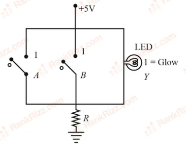
Following gates section is connected in a complete suitable circuit.
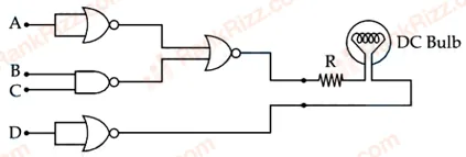
For which of the following combination, bulb will glow (ON) :
- A
- B
- C
- D
Every Semiconductor Electronics question JEE Main has set, grouped by the idea it tests rather than the order of the syllabus. 253 questions across 5 distinct ideas. Free to read, answer key on every one.
Questions
253
Distinct ideas
5
Share of marks
4.4%
Difficulty
EASY
A chapter is not one subject — it is a handful of procedures the examiner reuses. These are the ones Semiconductor Electronics questions actually test.
61–80 OF 253 · NEWEST FIRST
Following gates section is connected in a complete suitable circuit.
For which of the following combination, bulb will glow (ON) :
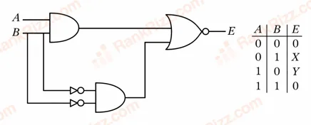
In the truth table of the above circuit the value of and are :
0, 0
1, 1
1, 0
0, 1
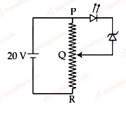
A potential divider circuit is connected with a dc source of 20 V, a light emitting diode of glow in voltage 1.8 V and a zener diode of breakdown voltage of 3.2 V. The length (PR) of the resistive wire is 20 cm. The minimum length of PQ to just glow the LED is _____ cm
In the given circuit, the current through the battery will be
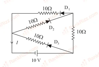
A
A
A
A
Which of the following statement is not correct in the case of light emitting diodes?
A. It is a heavily doped p-n junction.
B. It emits light only when it is forward biased.
C. It emits light only when it is reverse biased.
D. The energy of the light emitted is equal to or slightly less than the energy gap of the semiconductor used.
Choose the correct answer from the options given below:
C and D
A
C
B
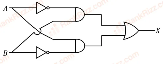
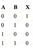
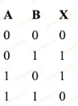
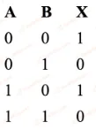
For the given logic gates combination, the correct truth table will be
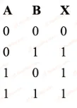
Name the logic gate equivalent to the diagram attached
NAND
AND
NOR
OR
The output for the inputs and of circuit is given by
Truth table of the shown circuit is:
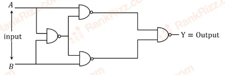
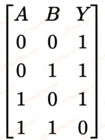
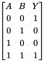
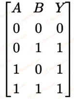
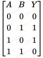
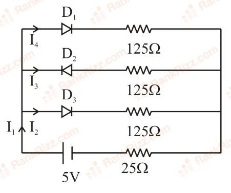
If each diode has a forward bias resistance of 25 in the below circuit, which of the following options is correct?
Given below are two statements: one is labelled as Assertion A and the other is labelled as Reason R.
Assertion A: Photodiodes are preferably operated in reverse bias condition for light intensity measurement.
Reason R: The current in the forward bias is more than the current in the reverse bias for a junction diode.
In the light of the above statement, choose the correct answer from the options given below :
A is false but R is true
Both A and R are true but R is NOT the correct explanation of A
A is true but R is false
Both A and R are true and R is the correct explanation of A
Given below are two statements: one is labelled as Assertion A and the other is labelled as Reason R.
Assertion A: Photodiodes are preferably operated in reverse bias condition for light intensity measurement.
Reason R: The current in the forward bias is more than the current in the reverse bias for a - junction diode.
In the light of the above statement, choose the correct answer from the options given below:
A is false but R is true
Both A and R are true but R is NOT the correct explanation of A
A is true but R is false
Both A and R are true and R is the correct explanation of A
The effect of increase in temperature on the number of electrons in conduction band and resistance of a semiconductor will be as:
Both and resistance decrease
Both and resistance increase
increases, resistance decreases
decreases, resistance increases
Choose the correct statement about Zener diode:
It works as a voltage regulator in reverse bias and behaves like simple p-n junction diode in forward bias
It works as a voltage regulator in both forward and reverse bias
It works a voltage regulator only in forward bias
It works as a voltage regulator in forward bias and behaves like simple p-n junction diode in reverse bias
In an n-p-n common emitter (CE) transistor the collector current changes from mA to mA for the change in base current from A and A, respectively. The current gain of transistor is _____.
The logic gate equivalent to the given circuit diagram is:
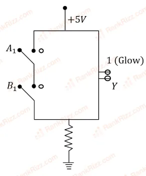
OR
NAND
NOR
AND
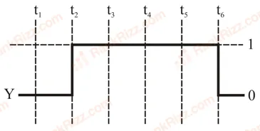
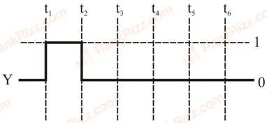
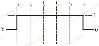
For the following circuit and given inputs and , choose the correct option for output 'Y'
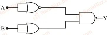
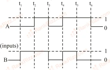
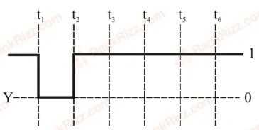
Given below are two statements:
Statement I: In a typical transistor, all three regions emitter, base and collector have same doping level.
Statement II: In a transistor, collector is the thickest and base is the thinnest segment.
In the light of the above statements, choose the most appropriate answer from the options given below.
Both Statement I and Statement II are correct
Both Statement I and Statement II are incorrect
Statement I is incorrect but Statement II is correct
Statement I is correct but Statement II is incorrect
Given below are two statements: one is labelled as Assertion A and the other is labelled as Reason R
Assertion A: Photodiodes are used in forward bias usually for measuring the light intensity.
Reason R: For a junction diode, at applied voltage the current in the forward bias is more than the current in the reverse bias for |V_z| > \pm V \geq |V_0| where is the threshold voltage and is the breakdown voltage.
In the light of the above statements, choose the correct answer from the options given below
Both A and R are true and R is correct explanation A
Both A and R are true but R is NOT the correct explanation A
A is false but R is true
A is true but R is false
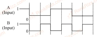
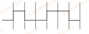
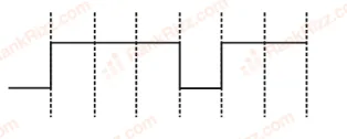
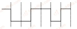
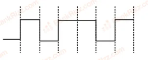
The output from a NAND gate having inputs A and B given below will be,
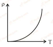
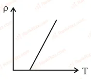
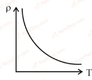
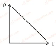
The resistivity of semiconductor varies with temperature. Which of the following curve represents the correct behaviour?
OTHER PHYSICS CHAPTERS