The conductivity of a semiconductor sample having electron concentration of electrons m, hole concentration of holes m, electron mobility of 2.0 m V s and hole mobility of 0.01 m V s is: (Take charge of an electron as C)
- A
1.83
- B
1.65
- C
1.20
- D
0.59
Every Semiconductor Electronics question JEE Main has set, grouped by the idea it tests rather than the order of the syllabus. 253 questions across 5 distinct ideas. Free to read, answer key on every one.
Questions
253
Distinct ideas
5
Share of marks
4.4%
Difficulty
EASY
A chapter is not one subject — it is a handful of procedures the examiner reuses. These are the ones Semiconductor Electronics questions actually test.
201–220 OF 253 · NEWEST FIRST
The conductivity of a semiconductor sample having electron concentration of electrons m, hole concentration of holes m, electron mobility of 2.0 m V s and hole mobility of 0.01 m V s is: (Take charge of an electron as C)
1.83
1.65
1.20
0.59
The current gain of a common emitter amplifier is 69. If the emitter current is 7.0 mA, collector current is:
69 mA
0.69 mA
6.9 mA
9.6 mA
For a common emitter configuration, if and have their usual meanings, the correct relationship between and is:
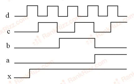
If a, b, c, d are inputs to a gate and x is its output, then, as per the following time graph, the gate is:

OR
NAND
NOT
AND
The temperature dependence of resistance of Cu and undoped Si in the temperature range 300 - 400 K is best described by:
linear increase for Cu, exponential decrease for Si
linear decrease for Cu, linear decrease for Si
linear increase for Cu, linear increase for Si
linear increase for Cu, exponential increase for Si
An unknown transistor needs to be identified as a npn or pnp type. A multimeter, with +ve and -ve terminals, is used to measure resistance between different terminals of transistor. If terminal 2 is the base of the transistor then which of the following is correct for a pnp transistor?
+ve terminal 2, -ve terminal 3, resistance low
+ve terminal 2, -ve terminal 1, resistance high
+ve terminal 1, -ve terminal 2, resistance high
+ve terminal 3, -ve terminal 2, resistance high
The ratio (R) of output resistance , and the input resistance in measurements of input and output characteristics of a transistor is typically in the range:
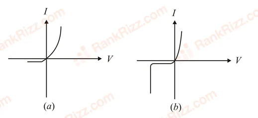
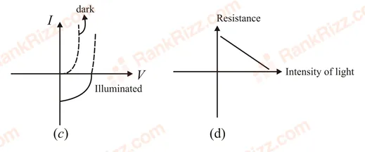
Identify the semiconductor devices whose characteristics are given below, in the order (a), (b), (c), (d):

Solar cell, Light dependent resistance, Zener diode, Simple diode
Zener diode, Solar cell, Simple diode, Light dependent resistance
Simple diode, Zener diode, Solar cell, Light dependent resistance
Zener diode, Simple diode, Light dependent resistance, Solar cell
A Zener diode with a breakdown voltage of 4 V is connected in series with a resistance to a battery of emf 10 V. The maximum power dissipation rating for the Zener diode is 1 W. The value of to ensure maximum power dissipation across the diode is
12
24
36
6
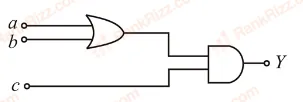
To get an output of 1 from the circuit shown in the figure the input must be:

The truth table given in fig. represents:
| A | B | Y |
|---|---|---|
| 0 | 0 | 0 |
| 0 | 1 | 1 |
| 1 | 0 | 1 |
| 1 | 1 | 1 |
OR-Gate
NAND-Gate
AND-Gate
NOR-Gate
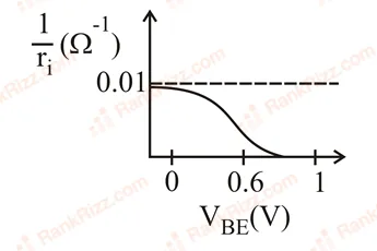
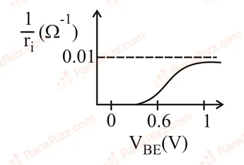
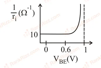
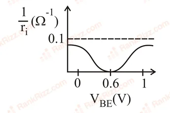
A realistic graph depicting the variation of the reciprocal of input resistance in an input characteristics measurement in a common emitter transistor configuration is:


In an unbiased p - n junction electrons diffuse from n-region to p-region because:
electrons travel across the junction due to potential difference
only electrons move from n to p region and not the vice - versa
electron concentration in n - region is more as compared to that in p - region
holes in p - region attract them
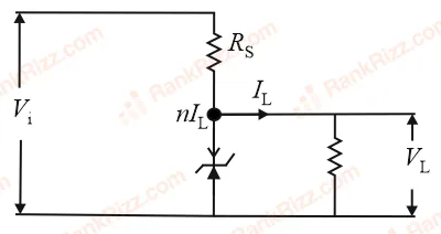
The value of the resistor, , needed in the DC voltage regulator circuit shown here, equals:

The current voltage relation of diode is given by mA, where the applied voltage V is in volts and the temperature T is in degree Kelvin. If a student makes an error measuring V while measuring the current of 5 mA at 300 K, what will be the error in the value of current in mA?
0.2 mA
0.02 mA
0.5 mA
0.05 mA
An n-p-n transistor has three leads A, B and C. Connecting B and C by moist fingers, A to the positive lead of an ammeter, and C to the negative lead of the ammeter, one finds large deflection. Then, A, B and C refer respectively to:
Base, emitter and collector
Base, collector and emitter
Emitter, base and collector
Collector, emitter and base
For LED's to emit light in visible region of electromagnetic light, it should have energy band gap in the range of:
0.1eV to 0.4eV
0.5eV to 0.8eV
0.9eV to 1.6eV
1.7eV to 3.0eV
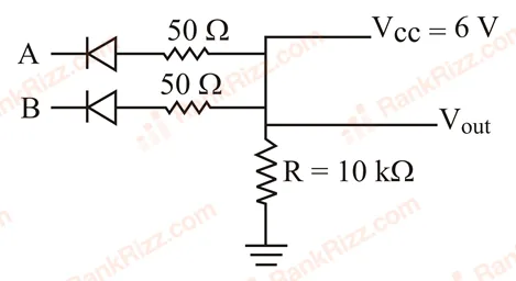
Given, A and B are input terminals. Logic 1 is > 5 V, Logic 0 is < 1 V. Which logic gate operation, the following circuit does?
Note: This question was awarded a bonus. C option changed.
OR gate
NOR gate
Output will always be one
XOR gate
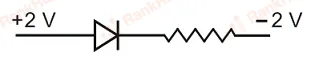
The forward biased diode connection is:


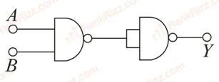
Identify the gate and match A, B, Y in the bracket to check.

OR (A = 1, B = 1, Y = 0)
XOR (A = 0, B = 0, Y = 0)
NOT (A = 1, B = 1, Y = 1)
AND (A = 1, B = 1, Y = 1)
OTHER PHYSICS CHAPTERS