RankRizzStart free

Semiconductor Electronics — JEE Main Previous Year Questions

Every Semiconductor Electronics question JEE Main has set, grouped by the idea it tests rather than the order of the syllabus. 253 questions across 5 distinct ideas. Free to read, answer key on every one.

Questions

253

Distinct ideas

5

Share of marks

4.4%

Difficulty

EASY

The ideas inside Semiconductor Electronics

A chapter is not one subject — it is a handful of procedures the examiner reuses. These are the ones Semiconductor Electronics questions actually test.

01Semiconductors: energy bands, intrinsic and extrinsicset 9×
02p-n junction diode and its characteristicsset 102×
03Diode circuits and rectifiersset 14×
04Zener diode, LED, photodiode and solar cellPractice questions coming soon
05Logic gates and digital circuitsset 85×
06Transistors (older syllabus)set 43×

Every Semiconductor Electronics question

41–60 OF 253 · NEWEST FIRST

JEE MAIN 2025 · 28 JAN S2p-n junction diode and its characteristicsTRANSCRIBED
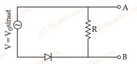
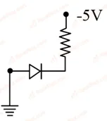
page6_img1


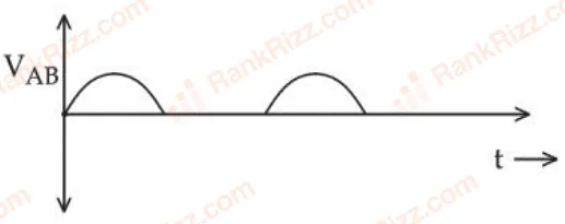
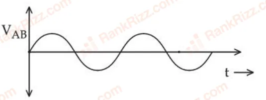
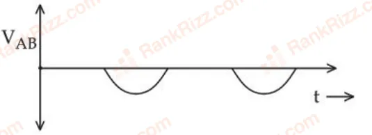
In the circuit shown here, assuming threshold voltage of diode is negligibly small, then voltage is correctly represented by :

  1. A

    would be zero at all times

  2. B
    page6_img2
  3. C
    page6_img3
  4. D
    page6_img4
JEE MAIN 2024 · 01 FEB S1p-n junction diode and its characteristicsTRANSCRIBED

In the given circuit if the power rating of Zener diode is mW, the value of series resistance to regulate the input unregulated supply is: 
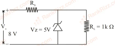
image
  1. A

    k

  2. B

  3. C

    k

  4. D

    k

JEE MAIN 2024 · 27 JAN S1p-n junction diode and its characteristicsTRANSCRIBED

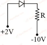
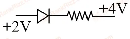
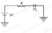
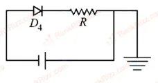
Which of the following circuits is reverse-biased?
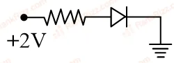
  1. A
    image
  2. B
    image
  3. C
    image
  4. D
    image
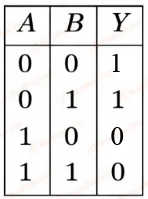
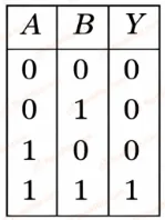
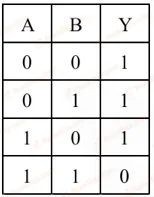
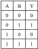
JEE MAIN 2024 · 27 JAN S2Logic gates and digital circuitsTRANSCRIBED

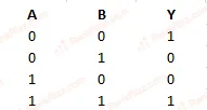
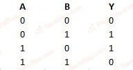
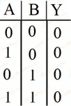
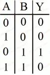
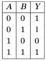
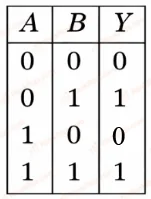
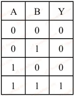
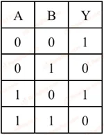
The truth table of the given circuit diagram is :
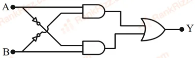
image
  1. A
    image
  2. B
    image
  3. C
    image
  4. D
    image
JEE MAIN 2024 · 30 JAN S2p-n junction diode and its characteristicsTRANSCRIBED

In the given circuit, the voltage across load resistance is:
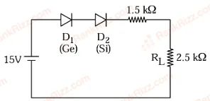
image
  1. A

    8.75 V

  2. B

    9.00 V

  3. C

    8.50 V

  4. D

    14.00 V

JEE MAIN 2024 · 31 JAN S2Logic gates and digital circuitsTRANSCRIBED

The output of the given circuit diagram is
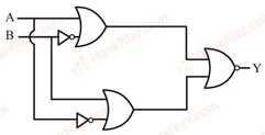
image
  1. A
    image
  2. B
    image
  3. C
    image
  4. D
    image
JEE MAIN 2024 · 04 APR S2Logic gates and digital circuitsTRANSCRIBED

Identify the logic gate given in the circuit:
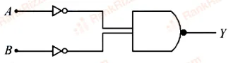
image
  1. A

    NAND-gate

  2. B

    AND gate

  3. C

    NOR gate

  4. D

    OR-gate

JEE MAIN 2024 · 05 APR S2Logic gates and digital circuitsTRANSCRIBED

The output of logic circuit given below is 0 only when 
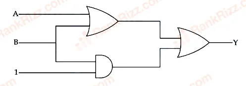
page3_img1
  1. A

  2. B

  3. C

  4. D

JEE MAIN 2024 · 06 APR S1Logic gates and digital circuitsTRANSCRIBED

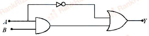
The correct truth table for the following logic circuit is :
image
  1. A
    image
  2. B
    image
  3. C
    image
  4. D
    image
JEE MAIN 2024 · 06 APR S2p-n junction diode and its characteristicsTRANSCRIBED

The acceptor level of a p-type semiconductor is . The maximum wavelength of light which can create a hole would be : Given .

  1. A

  2. B

  3. C

  4. D

JEE MAIN 2024 · 08 APR S1Logic gates and digital circuitsTRANSCRIBED

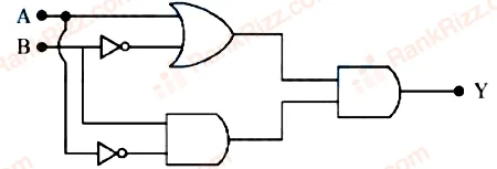
The output Y of following circuit for given inputs is :
image
  1. A

  2. B

    0

  3. C

  4. D

JEE MAIN 2024 · 09 APR S1p-n junction diode and its characteristicsTRANSCRIBED

A light emitting diode (LED) is fabricated using GaAs semiconducting material whose band gap is eV. The wavelength of light emitted from the LED is :

  1. A

    nm

  2. B

    nm

  3. C

    nm

  4. D

    nm

JEE MAIN 2024 · 09 APR S2p-n junction diode and its characteristicsTRANSCRIBED

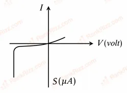
The characteristics of an electronic device shown in the figure. The device is:
image
  1. A

    a diode which can be used as a rectifier

  2. B

    a zener diode which can be used as a voltage regulator

  3. C

    a transistor which can be used as an amplifier

  4. D

    a solar cell

JEE MAIN 2024 · 04 APR S1Diode circuits and rectifiersTRANSCRIBED

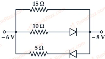
The value of net resistance of the network as shown in the given figure  is:
image
  1. A

  2. B

  3. C

  4. D

JEE MAIN 2024 · 01 FEB S2p-n junction diode and its characteristicsTRANSCRIBED

Conductivity of a photodiode starts changing only if the wavelength of incident light is less than 660 nm. The band gap of photodiode is found to be eV. The value of X is: (Given J s, C)

  1. A

    15

  2. B

    11

  3. C

    13

  4. D

    21

JEE MAIN 2024 · 29 JAN S1Diode circuits and rectifiersTRANSCRIBED

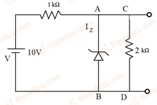
In the given circuit, the breakdown voltage of the Zener diode is V. What is the value of ?
image
  1. A

    mA

  2. B

    mA

  3. C

    mA

  4. D

    mA

JEE MAIN 2024 · 29 JAN S2Logic gates and digital circuitsTRANSCRIBED

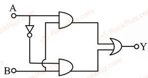
The truth table for this given circuit is:
image
  1. A
    image
  2. B
    image
  3. C
    image
  4. D
    image
JEE MAIN 2024 · 30 JAN S1p-n junction diode and its characteristicsTRANSCRIBED

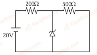
A Zener diode of breakdown voltage is used as a voltage regulator as shown in the figure. The current through the Zener diode is
image
  1. A

  2. B

  3. C

  4. D

JEE MAIN 2024 · 31 JAN S1Logic gates and digital circuitsTRANSCRIBED

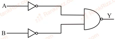
Identify the logic operation performed by the given circuit.
image
  1. A

    NAND

  2. B

    NOR

  3. C

    OR

  4. D

    AND

JEE MAIN 2024 · 04 APR S2p-n junction diode and its characteristicsTRANSCRIBED

Which of the diode circuit shows correct biasing used for the measurement of dynamic resistance of p-n junction diode:
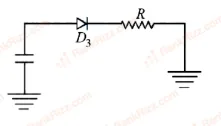
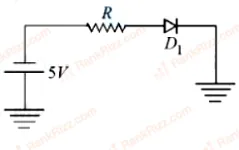
  1. A
    image
  2. B
    image
  3. C
    image
  4. D
    image